Modern industry runs on thin films. Solar cells. Flexible circuits. Nano-coatings. Wearable sensors. Every one of these technologies depends on a coating whose electrical resistance must be known — exactly. Too conductive or too resistive, and the product fails. Yet measuring that resistance accurately is one of the most underestimated challenges in materials testing.
Three Problems That Wreck Your Measurements
If you’ve ever tried to characterize a thin-film sample and ended up with fluctuating, inconsistent results, you’re not alone. Three root causes account for most of the trouble:
Problem 01
Getting the Current Wrong
Too little current and the signal disappears into noise — especially on high-resistance samples. Too much current heats the sample, changing resistance values and introducing non-ohmic contact effects. A smart instrument must adapt to each sample automatically.
Problem 02
50 Hz Power-Line Interference
Test leads act as an antenna, picking up 50 Hz mains interference. For low-resistance or very thin samples, that noise can match the signal magnitude — making accurate readings nearly impossible without active countermeasures.
Problem 03
Extreme Low-Resistance Samples
High-quality conductive coatings can have sheet resistance as low as 0.001 Ω/sq. Measuring at this scale demands sub-micron-ohm resolution — something most general-purpose instruments simply aren’t built for.
“Resistivity isn’t just a number — it determines whether your material is a conductor, a semiconductor, or an insulator. Getting it wrong means shipping the wrong product.”
The Two Parameters That Matter Most
Every thin-film electrical characterization workflow ultimately comes down to two core measurements:
Sheet Resistance (Rs)
Expressed in Ω/sq (ohms per square), Rs captures the electrical conductivity of the thin layer independent of its thickness. It determines performance of transparent conductive films, thin-film resistors, and anti-static coatings. The four-probe method eliminates contact resistance so you measure the true material value.
Resistivity (ρ)
Expressed in Ω·cm or Ω·m, resistivity is the material’s intrinsic resistance regardless of geometry. It tells you whether silicon is p-type or n-type, whether a coating holds charge or bleeds it off. Accurate measurement requires accounting for polarization effects and skin depth.
The Solution
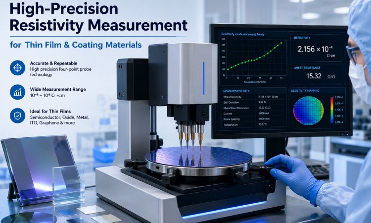
HT3542Y / HT3545Y Four-Probe Square Resistance Tester
Hope Instrument’ HT3542Y and HT3545Y were designed from the ground up to address each of the challenges above. Built on the four-probe measurement principle — the gold standard for thin-film characterization — the series delivers professional-grade accuracy without the complexity of a research-lab setup.
|
📊 Multi-Parameter Display Resistance, surface resistance, resistivity, and conductivity — all four displayed simultaneously in real time. No mode-switching, no recalculation. |
🎯 Ultra-High Resolution Minimum resolution of 0.01 μΩ across 0 to 1,200 MΩ. Handles conductive metals and near-insulating coatings equally. |
|
🔄 Dual-Direction Averaging Automatically measures and averages forward and reverse currents, correcting probe drift errors and boosting long-term stability. |
🔌 RS232 + LAN Interfaces Standard connectivity with professional host software for real-time data logging and full traceability. |
▪ Key Specifications
| Parameter | Specification |
|---|---|
| Measurement Range | 0 – 1,200 MΩ |
| Minimum Resolution | 0.01 μΩ |
| Resistance Accuracy | Maximum 0.01% |
| Surface Resistance Accuracy | Maximum 2% |
| Measurement Method | Four-probe (eliminates contact resistance) |
| Current Correction | Dual-direction averaging algorithm |
| Optional Probes | Direct discharge & rectangular configurations |
| Connectivity | RS232, LAN; compatible host computer software |
Real-World Application: Silicon Wafer Testing
A high-tech enterprise developing single-polished silicon wafer materials needed to characterize both sheet resistivity and bulk resistivity on wafers 525 μm thick. Requirements: extreme accuracy, zero sample damage from probe pressure, and repeatable results across production batches.
The HT3542Y/3545Y addressed all of these directly. Four-probe approach eliminated contact resistance. Probe pressure control protected brittle silicon. Dual-direction current averaging corrected probe drift — delivering consistent, traceable data across the entire batch.
Industry context: Silicon wafer resistivity spans 0.001 to 10,000 Ω·cm depending on doping level. Accurately distinguishing p-type from n-type, or characterizing doping uniformity, requires exactly the kind of wide-range, high-resolution measurement the HT3542Y/3545Y delivers.
Who Should Be Using This Instrument
|
Semiconductors Resistivity mapping, doping characterization, ion implantation QC |
Solar & Energy TCO sheet resistance, ITO/AZO uniformity, conductive grid testing |
Flexible Electronics Conductive inks, printed circuits, roll-to-roll film uniformity |
|
Nano-Coatings Anti-static, EMI shielding, and metallic decorative coatings |
R&D & Academic Labs Materials characterization, new conductive material development, QC benchmarking for novel thin-film technologies |
|
Why Measurement Method Matters as Much as Accuracy
Even the most accurate instrument gives wrong results if the method is incorrect. In a two-probe setup, contact resistance adds directly to the measured value — for thin films, this can equal or exceed the film’s own resistance. The four-probe method uses separate probe pairs for current injection and voltage sensing: voltage probes draw negligible current, so their contact resistance contributes essentially nothing.
The HT3542Y/3545Y goes further with dual-direction averaging: measuring with current in both directions and averaging the results cancels thermoelectric offset voltages and probe drift — error sources most instruments ignore entirely.
Conclusion
Thin film resistivity measurement looks simple on paper — apply a current, measure a voltage, calculate resistance. In practice, the physics of ultra-thin materials, lab electromagnetic environments, and industrial QC demands make it one of the most technically nuanced measurements in materials testing.
The HT3542Y/3545Y series exists to close that gap: professional four-probe measurement with the resolution, accuracy, and flexibility that semiconductor, coating, and thin-film applications actually require. The right measurement foundation isn’t optional — it’s the difference between product success and field failure.
Hope Instruments
Ready to Characterize Your Thin Films?
We supply the HT3542Y and HT3545Y series globally. Speak with our technical team about your sample requirements, probe configuration, and workflow integration.